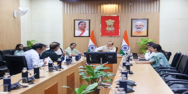
Bhubaneswar, 12 August (H.S.): In a major boost to India's semiconductor ecosystem, Union Education Minister Shri Dharmendra Pradhan has welcomed the Central Cabinet’s approval for setting up two advanced semiconductor units in Odisha under the India Semiconductor Mission, calling it a “semiconductor revolution in the making.”
Sharing the development on social media, Shri Pradhan said that the Cabinet, under the leadership of Prime Minister Shri Narendra Modi, has approved the establishment of an integrated compound semiconductor fabrication and ATMP (Assembly, Testing, Marking and Packaging) facility in Bhubaneswar, and a vertically integrated advanced packaging and embedded glass substrate unit in Info Valley, Khordha.
He stated that these projects mark a significant milestone in positioning Odisha as a vital player in the global semiconductor innovation and manufacturing value chain. They are also crucial steps towards making India a self-reliant semiconductor hub.
The proposed semiconductor fab and ATMP unit will be set up with an investment of ₹2066.70 crore, while the advanced packaging and embedded glass substrate unit will attract ₹1943.53 crore in investment. Both units are expected to contribute significantly to strengthening India’s semiconductor ecosystem.
“These facilities will enhance our chip design capabilities, support modern electronics manufacturing, and foster technological advancement,” said Shri Pradhan. He also highlighted that the projects will catalyse the growth of ancillary industries in Odisha, creating large-scale direct and indirect employment opportunities.
Shri Pradhan emphasised that the initiative aligns with the vision of Atmanirbhar Bharat and the long-term goal of transforming India into a semiconductor manufacturing powerhouse. He credited the proactive policy framework, including Odisha's amended Semiconductor Manufacturing and Fabless Policy, for making the state an attractive destination for high-value tech investments.
---------------
Hindusthan Samachar / Monalisa Panda
13 Aug 2025